

Integrated photonics aims to place more optical function into compact, repeatable circuits, yet high-speed modulation remains a demanding element. They need strong electrical control of light without excessive voltage, loss, footprint, or distortion. Materials and processes that improve this balance attract attention because they can influence driver power, optical budget, and package complexity simultaneously.
At the material level, thin-film lithium niobate brings a well-known electro-optic material into waveguide structures compatible with smaller circuits and high-frequency electrodes. The platform can support intensity, phase, and IQ functions, including multi-channel devices.
Its potential is significant, but the result still depends on lithography, etching, coupling, electrode design, packaging, and statistical process control. Design kits and compact models are checked against measured devices, enabling circuit and package teams to predict behavior before committing expensive masks or interposers.
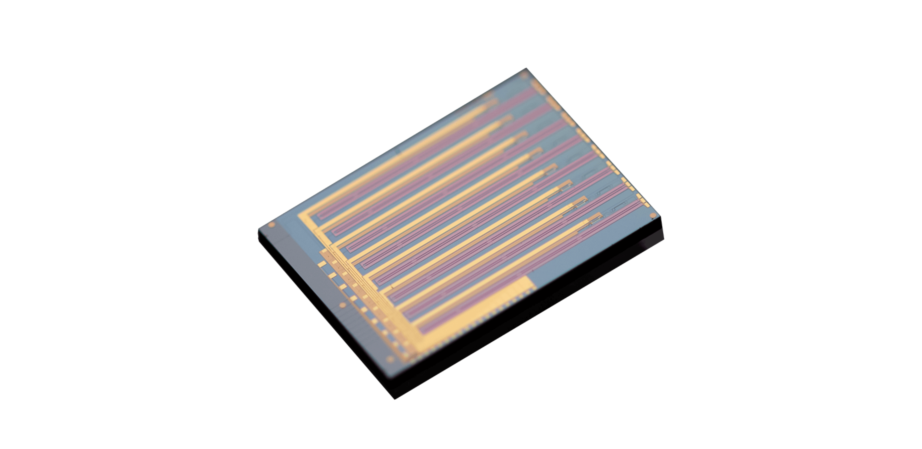
The current product set of TFLN chips spans 70 to 110 GHz and include devices for 800G, 1.6T, 3.2T, and coherent ZR formats. They consider these data as evidence of application direction, then ask how measured voltage, insertion loss, extinction, channel uniformity, and assembly interfaces compare with the requirements and manufacturing capabilities of their intended optical engine.
Thin-Film Lithium Niobate Addresses a Difficult Modulation Trade-Off
The interest in TFLN chips begins with electro-optic efficiency. Strong interaction can provide useful modulation at practical voltage while supporting wide bandwidth. For their system, this may reduce driver swing or improve signal margin.
They verify the delivered response because electrodes, substrate modes, connectors, and package transitions can limit the advantage predicted by the material alone. Inside a dense optical path, photonic integrated circuits must protect the optical budget. Waveguide propagation, couplers, splitters, crossings, and modulation sections all contribute loss.
They request a clear breakdown between intrinsic device loss and coupling loss, then model laser power and receiver sensitivity across temperature and aging. A compact die is not efficient if it transfers burden to the source. Linearity and extinction matter differently by architecture.
Direct-detection links need clean intensity levels, while coherent systems require balanced amplitude and phase paths. They examine transfer curves, bias sensitivity, electrode matching, and channel isolation under large-signal drive. Small-signal bandwidth is one part of the evidence needed for a high-order communication waveform.
Integration Value Depends on Circuit Function and Interface Design
One listed 3.2T DR8 option reaches 110 GHz with insertion loss below 14 dB including coupling, differential half-wave voltage below 1.5 V, and DC extinction above 25 dB. These TFLN chips illustrate how multi-lane integration can combine fast response with lower drive, though the full module must validate lane uniformity and total power.
Coherent photonic integrated circuits integrate more optical operations. A 70 GHz PDMIQ chip for 800G and 1.6T ZR is listed below 7 dB loss, below 4.5 V differential half-wave voltage, and above 25 dB extinction. They compare it according to the functions included, required bias controls, and the DSP or driver architecture it enables.
A bare 110 GHz intensity-modulator die offers another integration route, with loss below 5 dB, voltage below 3 V, and extinction above 20 dB. Custom packaging can optimize footprint or interfaces, but it transfers fiber coupling, RF launch, thermal design, reliability, and test responsibility to their organization or manufacturing partner.
That responsibility must be priced explicitly. They also examine substrate availability and process concentration, because a technically appropriate platform may carry geographic or capacity risks that affect long-term sourcing.
Manufacturing Maturity Determines the Pace of Adoption
Adoption of TFLN chips depends on repeatable fabrication across wafers and lots. They request statistical distributions for bandwidth, voltage, loss, extinction, and channel balance, plus information about wafer mapping and screening. Typical values do not reveal tail behavior that may govern multi-channel yield or force excessive module guard bands.
For photonic integrated circuits entering volume, packaging capacity can become the limiting step. Fiber arrays, precision alignment, RF interposers, wire bonds or bumps, adhesives, and thermal materials each require controlled processes.
They inspect ownership of those processes, correlation between partners, and notification rules for changes that could alter high-frequency or optical performance. Lifecycle readiness includes design rules, models, reference structures, failure analysis, and roadmap compatibility.
They prefer suppliers who can explain observed variation and support root-cause work, rather than replace failed samples. Sustained engineering cooperation helps the platform develop and protects product teams when early assumptions meet the complexity of scale. Adoption gates include a fallback architecture, protecting the product schedule while the newer platform completes reliability and scale evidence.
From a system viewpoint, thin-film lithium niobate is gaining attention because it addresses a difficult combination of modulation speed, drive voltage, optical loss, and circuit density.
The material platform creates useful design possibilities, but its commercial value depends on how well fabrication, coupling, packaging, control, and testing preserve those advantages in complete assemblies. They compare candidate chips through common reference planes and application-specific prototypes.
Multi-lot characterization, reliability testing, yield analysis, and supplier audits then determine whether the platform fits their production roadmap. The resulting evidence links laboratory capability with repeatable production performance.
This measured sequence is more useful than assuming that an early-stage material platform automatically produces a lower-risk product. For comparative evaluation, the supplier presents several direct-detection and coherent chip configurations that can enter such an assessment.
Interest in TFLN becomes actionable when system margin, package route, process variation, and lifecycle support are compared together. Representative Liobate data can anchor that comparison and keep platform expectations tied to delivered behavior.
